Basic Science of Nanomaterials
Shaun Williams, PhD
Prelude to Basic Science of Nanomaterials

- What do the above items all have in common?
- All of them derive some special property and utility from nanoscale materials.
- Ordinary elements and inorganic compounds such as gold, silver, \(\chem{TiO_2}\), \(\chem{SiO_2}\) acquire different properties when their dimensions are between 1 and 100 nm.
Physics and Length Scales - Cavity Laser, Coulomb Blockade, Nanoscale Magnets
- The special properties of nanomaterials do not derive from different laws of physics.
- The physics of electrons, atoms, and photons naturally produce characteristic length scales.
- For instance the Bohr radius of an electron in silicon is about 4 nm
- When objects become small relative to these characteristic lengths, the physical properties change in interesting ways
- Materials that exist at these lengths scales are called mesoscopic (meso = between, scopic = size)
- This length scale is different for different kinds of properties
The Cavity Laser
- A vertical cavity surface-emitting laser (VCSEL) is a semiconductor-based device that emits light in the vertical direction relative to plane of the chip.
- The VCSEL is basically a light-emitting diode but has two special features
- the refractive index of the semiconductor is modulated above and below the junction to make Bragg mirrors which reflect light emitted in the junction
- The junction itself consists of a thin "quantum well" layer of (In, Ga)As semiconductor which has a smaller band gap than the surrounding (Al, Ga)As layers
Effect of the Quantum Well
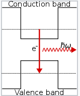
- Note that if electrons are injected into the thin (In,Ga)As layer, they do not have enough energy to climb out of the well and into the surrounding conduction band
- Particles in such a small well behave as a particle-in-a-box (PIB)
- The kinetic energy of a PIB is given as \[ KE = \frac{h^2 n^2}{8mL^2} \]
Quantum Well Energy Transitions
- We can calculate the energy difference between the lowest (\(n=1\)) and next lowest (\(n=2\)) levels, which is inversely proportional to the square of the thickness (\(L\)) of the (In,Ga)As layer
- In this calculation, the mass of the electron in (In,Ga)As is about 7% of the electron rest mass
- with an 8 nm thick layer \[ \begin{align} E &= \frac{\left( 2^2 - 1^2 \right) \left( 6.626 \times 10^{-34}\,J \cdot s\right)^2}{8\cdot 0.07 \cdot \left( 9.1 \times 10^{-31}\, kg \right) \left( 8 \times 10^{-9}\,m \right)^2} \\ &= 4.0 \times 10^{-20}\, J = 0.25\,eV \end{align} \]
- Thus, the cavity will have a resonant energy of 0.25 eV which corresponds to energy in the infrared (\(\lambda \approx 5000\, nm\))
Coulomb Blockade
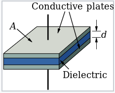
- A capacitor is a macroscopic device that stores electrical charge
- When a voltage is applied, a capacitor develops a charge, \( C=\frac{Q}{V} \)
- The magnitude of the capacitance C is determined by the permittivity \( \varepsilon \) and the dimensions of the dielectric layer, A and d
- The work done in charging the capacitor is \[ \begin{align} E &= \int_0^Q V(q) dq = \int_0^Q \frac{q}{C} dq = \frac{1}{2}\frac{Q^2}{C} \\ &= \frac{1}{2}CV^2 = \frac{1}{2}VQ \end{align} \]
Very Small Capacitors
- What happens to a capacitor when we make it very small?
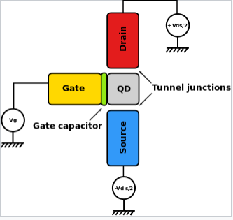
- This is of particular interest in a device called a single electron transistor (shown below)
- The metallic gate lead is separated from a "quantum dot" (metal or semiconductor particle) by a thin dielectric layer
- The energy needed to charge it by a single electron (\(Q=e\)) is \[ E=\frac{e^2}{2C} \]
The Result?
- The result of this is that a voltage of about 200 mV is needed to charge the quantum dot by a single electron
- Devices just 10 times larger reduce this charging voltage to 20 mV which is smaller than thermal energy
- Thus devices larger than 5-6 nm, individual charging events are washed out at room temperature by thermal fluctuations
- This has resulted in research being conducted using these as ultra-sensitive electrometers and single-molecular chemical sensors since a tiny change in the electrostatic environment of the dot can switch it on and off
Nanoscale Magnets
- Ferro- and ferrimagnetic materials such as iron and chromium oxide are used for digital storage in hard disks
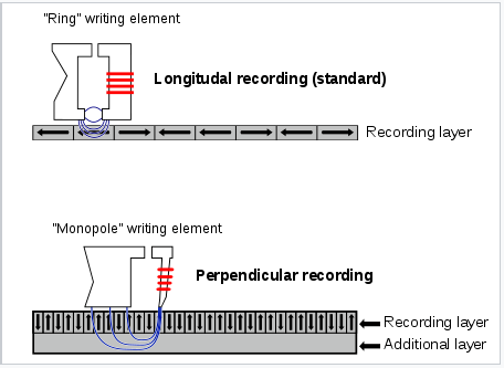
- Individual memory bits, which can be oriented perpendicular or parallel to the plane of the disk (shown below) store a logical "0" or "1" depending on the orientation of their magnetic dipole
- a 2.5" hard drive can store 1 TB of information using rod-shaped magnetic grains that are approximately 0.5 μm long
Can't we make them smaller?
- We can actually synthesize materials with dimensions of only a few nanometers
- The reason we can't immediately use those to increase storage capacity is that the energy needed to flip the magnetization is strongly size-dependent
- For a ferro- or ferrimagnet this energy is equal to \(Mr^3\) where M is the magnetic energy per unit volume and r is the characteristic dimension of the magnetic grain
- For typical materials, this energy is in the kT region when r is about 3-5 nm
- These are then called superparamagnetic meaning that they still have a large magnetic moment because of the ordering of the spins, but they do not retain a permanent polarization in the absence of an applied magnetic field
- Superparamagnetic particles are not useful for magnetic memory but they are used in things such as ferrofluids, magnetic resonance imaging (MRI), and other medical diagnostic and therapeutic applications.
Ferrofluid
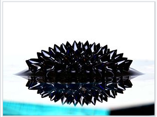
The following ferrofluid contains superparamagnetic \(\chem{Fe_3O_4}\) nanoparticles coated with oleic acid and suspended in oil.
Semiconducting Quantum Dots
- One of the most fascinating and well-studied mesoscopic effects occur with semiconducting particles of various shapes when one or more of their dimensions is in the range of a few nanometers
- These so-called "quantum dots" (0D), "quantum rods" (1D), and "nanosheets" (2D) acquire striking new electronic and optical properties
- The synthesis of quantum dots give essentially perfect crystals of a few thousand atoms
- These crystals can be capped with an epitaxial layer of ligands or by a shell of wider bandgap semiconductor
Behavior of Quantum Dots
- Electron-hole pairs formed by excitation of the core semiconductor are confined there are cannot reach the external surface of the particle where they would be trapped or recombine thermally
- Thus, the quantum yield for band gap emission of the semiconductor quantum dots is typically high giving rise to bright emission colors
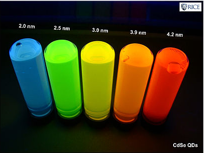
- Below are the emission colors of CdSe nanoparticles of different sizes
Size Dependence of Emission Colors
- The size-dependence of the emission color comes primarily from a particle-in-a-box effect
- The electron and hole that are created when the quantum dot absorbs light are bound together as an exciton by the confines of the "box"
- Louis Brus used first-order perturbation theory to determine that the bandgap of a semiconductor quantum dot is given approximately by \[ E_{gap} = E_{gap,bulk} + \frac{h^2}{8\mu R^2} - \frac{1.8e^2}{4R\pi \varepsilon \varepsilon_0} \] where R is the particles radius, μ is the electron-hole reduced mass, and ε is the dielectric constant of the semiconductor
Synthesis of Semiconductor Nanocrystals
- Early work on the quantum size effect in semiconductions used simple metathesis reactions in the synthesis
- For example, CdSe and PbS can be precipitated at ambient temperature by the reactions: \[ \begin{align} \chem{CdCl_2(aq) + H_2Se(g)} &\rightarrow \chem{CdSe(s) + 2HCl(aq)} \\ \chem{Pb\left( NO_3 \right)_2(aq) + H_2S(g)} &\rightarrow \chem{PbS(s) + 2HNO_3(aq)} \end{align} \]
Model of Colloidal Lead Sulfide Nanoparticle
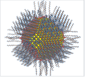
- Above is a complete atomistic model of a 5 nm diameter colloidal lead sulfide nanoparticle
- This particle possesses surface passivation by oleic acid, oleyl and hydroxyl groups
Restricting Growth
- The growth of the particles was restricted by carrying out the reactions in different matrices
- polymer films, silicate cages of zeolites, etc.
- Capping ligands were also sometimes used to limit particle growth
- While these reactions did produce nanoparticles, a broad distribution of particle sizes was obtained
- These particles were also unstable to Ostwald ripening in which large particles grow at the expense of smaller ones
- A lock of good samples prevented detailed studies and the development of applications for semiconductor quantum dots.
A New Synthesis Method
- In the 1990's, Murray, Norris, and Bawendi introduced the first non-aqueous, controlled growth process for II_VI semiconductor quantum dots
- The keys to this synthesis were
- use of non-aqueous solvents and capping ligands to stabilize the products against ripening
- carry out the reaction at high temperature to ensure good crystallinity
- separate the steps of particle nucleation and growth to obtain particles of uniform size
Murray, Norris, and Bawendi Synthesis Scheme

- synthesis is carried out in a coordinating, high boiling solvent that is a mixture of trioctylphosphine (TOP) and trioctylphosphine oxide (TOPO).
- At the beginning, a selenium source, typically bis(trimethylsilyl)selenium, \(\chem{\left[\left( CH_3 \right)_3 Si\right]_2 Se}\), dissolved in TOP is rapidly injected into the reaction mixture
- The reaction causes a rapid burst of nanoparticle nucleation, but the temperature also drops as cold solvent is injected and so the nucleation event ends quickly.
More on this Synthesis
- The cooled solution now contains nanocrystal seeds. It is supersaturated in TOPO-Cd and TOP-Se, but particle growth proceeds slowly until the solution is heated again to the growth temperature, about 250°C.
- Particle growth and size-focusing occurs because small particles require less added material to grow by an amount ΔR than larger particles.
- The size distribution can then be narrowed further by adding a non-solvent such as hexane to the cooled reaction mixture causing the largest particles precipitate first, followed by smaller particles.
- Because the nanoparticles are capped with a ligand shell of TOP, they can be re-suspended in organic solvents once they are size-separated.
Other Synthesis Methods
- Other synthesis methods have since been developed such as
- vapor-liquid-solid (VLS)
- solution-liquid-solid (SLS)
- chemical vapor deposition (CVD)
Surface Energy
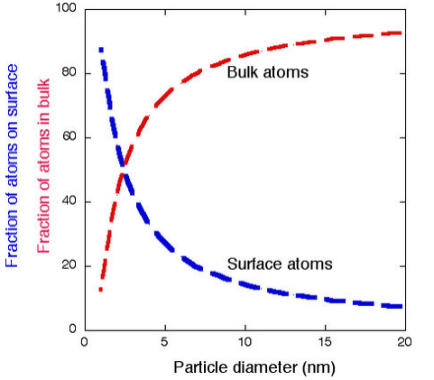
- Nanoparticles have a substantial fraction of their atoms on the surface (see below)
- The high surface area to volume ratio is important factor in many physical properties
Surface Energy
- The surface energy is always positive and is connected with the chemistry of all surfaces
- This is the (thermodynamically unfavorable) energy of making "dangling bonds" at the surface
- Atoms at the surface are under-coordinated, and because breaking bonds costs energy, surface atoms always have higher energy than atoms in the bulk
- For example, a gold atom in bulk face-centered cubic Au has 12 near neighbors, but a gold atom on the (111) surface of the crystal (the most dense crystal plane of gold) has six nearest neighbors in-plane and three underneath, for a total of 9
- We might expect the surface energy of this crystal face to be a little less than \( \frac{3}{12} = \frac{1}{4} \) of the bonding energy of bulk Au, and this is in fact a fairly good rule of thumb for many materials.
Effects of Surface Energy Differences
- Various properties change with this surface energy
- The melting point of nanoparticles can be hundreds of degrees below that of the bulk material
- Additionally, nanoparticles have lower boiling points, higher vapor pressures, higher solubility, and higher reactivities
Nanoscale Metal Particles
- Nanoscale metal particles have been the subject of intense research over the past 20 years, especially because of their unusual optical, magnetic, and catalytic properties.
- The synthesis of metal nanocrystals in various shapes has become increasingly sophisticated and rational, like the synthesis of semiconductor nanocrystals described previously.
- The interesting optical properties of nanocrystalline Au, Ag, Cu, and a number of other metals, derive from the collective oscillation of their valence electrons, a phenomenon known as plasmon resonance.
Plasmon Resonance
- Remember that in these metals, the electron mean free path is much longer than the atom so the valence electrons feel only the average positive charge of the atomic cores
- Light impinging on the metal acts as an oscillating electric field, pushing and pulling on the valence electrons at the characteristic frequency of the light wave
- The electrons, pushed away from their equilibrium positions, feel a restoring force that is proportional to their displacement and their motion can be described by Hooke's Law: \[ F=kx \]
- In the case of the plasmon resonance, the spring constant k is proportional to the number density of valence electrons n: \[ k=\frac{ne^2}{\varepsilon_0} \]
Plasmon Resonance Frequency
- The resonant frequency of the plasma oscillation is given by: \[ \omega_p = \left( \frac{k}{m} \right)^\frac{1}{2} = \left( \frac{ne^2}{m_e \varepsilon_0}\right)^\frac{1}{2} \]
- For most metals, the plasmon resonance is in the ultraviolet part of the spectrum, but for a few metals like Au, Ag, and Cu it is in the visible.
- The Lycurgus cup (4th century Roman glass) derives its unique coloration from noble metal nanoparticles.
- The cup is red in transmitted light and green in scattered (reflected) light.

Localized Surface Plasmon Resonance (LSPR)
- For metal particles that are much smaller than the wavelength of light, this effect is called the localized surface plasmon resonance
- There are three important consequences of the LSPR effect:
- The local electric field of the incoming light wave is greatly enhanced at the particle surface. This gives rise to huge enhancement factors in optical processes such as Raman scattering and fluorescence.
- Near the plasmon resonance frequency, metal nanocrystals absorb and scatter light very strongly. This makes them brightly reflective, and the strong light absorption can be exploited for light-induced local heating.
- The plasmon frequency is sensitive to the refractive index of the particle's surroundings
Plasmonic Gold Nanoparticles
Theory of Light Scattering and Absorption by Metal Nanoparticles
- The valence electrons in metal nanoparticles oscillate in the electric field of a light wave
- The theory for spherical particles is relatively simple and in fact was worked out over 100 years ago by German physicist Gustav Mie.
- Mie considered the interaction of a spherical particle with a uniform electric field, E, oscillating at angular frequency \( \omega = 2\pi f\).
- This is a good approximation when the particle diameter is much smaller than the wavelength of light
- The particle is embedded in a uniform, insulating material (e.g. a solvent) that has a dielectric constant \(\varepsilon_{diel}\) - for insulators, \(\varepsilon_{diel}\) is a positive real number.
A Brief Aside Concerning Dielectric Constants, \(\varepsilon\)
- The index of refraction (\(n\)) of a transparent material describes how the velocity of light is slowed in the medium compared to vacuum \[ n=\frac{c}{v_n} \] where \(v_n\) is the speed of the light in that medium
- This results in the standard optical effect of light refraction
- The index of refraction of a material to its index of refraction \[ n = \sqrt{\varepsilon} = \frac{c}{v_n} \]
- So, we could say that the speed of light in a medium with a dielectric constant of \(\varepsilon\) is \( v = \frac{c}{\sqrt{\varepsilon}} \)
Dielectric Constants of Metals
- The dielectric constant ε of a metal is actually a complex number:
\[ \varepsilon = \varepsilon' + i \varepsilon'' \]
- ε' is the real part and is related to the refraction of light
- ε" is the imaginary part and is related to light absorption
- Both ε' and ε" are dependent on the frequency of the light
- For metals near the plasmon resonance frequency, ε' is typically a negative number.
Light Absorption and Scattering
- The cross-section for absorption of the light wave by the particle is: \[ \sigma_{absorption} = \frac{9\omega}{c} \varepsilon_{diel}^\frac{3}{2} V\frac{\varepsilon_{metal}''}{\left( \varepsilon_{metal}'+2\varepsilon_{diel}\right)^2 + \left( \varepsilon_{metal}'' \right)^2} \]
- The cross-section for scattering is: \[ \sigma_{scattering} = \frac{3}{2\pi} \left( \frac{\omega^4}{c}\right) \varepsilon_{diel}^2 V^2 \frac{\left( \varepsilon_{metal}'-\varepsilon_{diel}\right)^2 + \left( \varepsilon_{metal}'' \right)^2}{\left( \varepsilon_{metal}'+2\varepsilon_{diel}\right)^2 + \left( \varepsilon_{metal}'' \right)^2} \]
- The sum of these two is the cross-section for extinction: \[ \sigma_{extinction} = \sigma_{absorption} + \sigma_{scattering} \]
- These cross-sections become large when \(\varepsilon_{metal}' \simeq -2\varepsilon_{diel}\)
Changing Effects
- The cross-sections become large when \(\varepsilon_{metal}' \simeq -2\varepsilon_{diel}\)
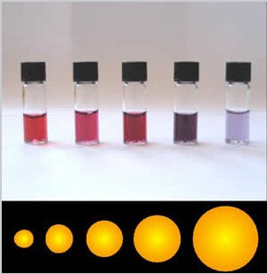
- For 15 nm diameter gold nanoparticles in water, this happens at about 580 nm, resulting in the characteristic wine-red color of colloidal gold solutions.
- It is important to note that the cross-section for scattering is proportional to the square of the volume of the particle, \(V^2\), whereas the absorption is proportional to \(V\)
- This means that very small gold particles (< 5 nm) are strongly absorbing but not strongly scattering.
- Larger particles (>30 nm) scatter light very strongly
- Depending on the application, therefore, we choose larger or smaller particles
Use in Medicine
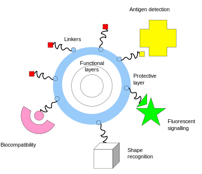
- One of the key complementary properties of noble metal nanoparticles is the ease with which they can be covalently conjugated with polymers or small molecules, typically via thiol or amine bonds at their surface
- This imparts biological recognition properties to the particles that enables them to bind to specific biomolecular targets
One of the First Nanoparticle Sensors
- Functionalization of gold nanoparticles with thiol-terminated single-stranded DNA was developed by the Mirkin group at Northwestern University
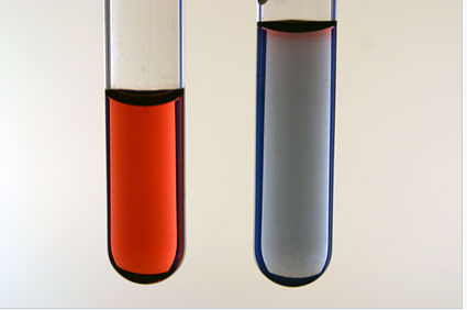
- DNA-coated nanoparticles have the characterstic wine-red plasmonic color of spherical nano-gold
- However, when these particles are linked together by a complementary DNA strand, the resonance frequency shifts, resulting in a blue color
Other Applications
- Spherical nucleic acid particles which can easily penetrate cell membranes and can report on the chemistry happening inside living cells.
- An important property of gold nanoparticles in these applications is their ability to quench the fluorescence of reporter molecules that are near their surface
- Nucleic acid strands that contain a hairpin loop can position fluorescent molecules near the gold surface, where their fluorescence is turned off by nanoparticle quenching
- Hybridization of these sequences to target RNA or DNA causes the fluorescence to turn on by moving the fluorescent molecule away from the nanoparticle surface
- These so called "nanoflares" can thus signal the up- or down-regulation of specific genes inside cells
- These nanoflares can be used to detect markers for infectious diseases and cancers
/